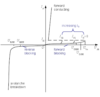
A thyristor can be switched from a non conducting state to a conducting state in several ways-
Forward Voltage Triggering (High Voltage)
When anode to cathode forward voltage is increased with gate circuit open, the leakage current of the thyristor increases. Due to internal current multiplication taking place inside, this current increases. As soon as the forward voltage reaches the breakover voltage (VBO), the reverse biased junction J2 will have an avalanche breakdown.
At this voltage, thyristor changes from OFF state to ON state characterized by a low forward voltage across it with large forward current. This type of turn ON may be destructive and should be avoided.Thermal Triggering ( Temperature Triggering)
Like any other semiconductor, the width of depletion layer of a thyristor decreases on increasing junction temperature. When the temperature of thyristor is high, there is an increase in the number of electron-hole pairs which increases the leakage current. This increase in leakage current causes increase in current amplification factor ∝1 and ∝2. Due to the regenerative action, ∝1+∝2 may tend to be unity and the thyristor may be turned ON. This is called thermal triggering of thyristor. This type of turn ON may cause thermal runaway and is normally avoided.
Light Triggering (Radiation Triggering)
If light of adequate frequency and intensity is allowed to strike the thyristor junction, then the photons will strike the electrons and increase the number of electron-hole pairs. This leads to instantaneous flow of current within the device and the triggering of the device. For light triggering to occur, the device must have high value of rate of change of voltage (dV/dt).
dV/dt Triggering
With forward voltage across the anode and cathode of a device, junction J1 and J3 are forward biased whereas the junction J2 becomes reverse biased. This reverse biased junction J2 has the characteristic of a capacitor due to charge existing across the junction. If a forward voltage is suddenly applied, a charging current will flow tending to turn ON the device. If the voltage impressed across the device is denoted by V, the charge by Q and capacitance by Cj then,
The rate of change of junction capacitance may be negligible as the junction capacitance is almost constant. If the rate of change of voltage across the device is large, the device may turn ON even though the small voltage appearing across the device is small.
Gate Triggering
This is the most commonly used method for SCR triggering. The injection of gate current by applying positive gate voltage between the gate and cathode terminals turn ON the SCR much before the specified breakover voltage. The conduction period of the SCR can be controlled by varying the gate signal within the specified value of maximum and minimum gate current. Three types of signals can be used for triggering the SCR using gate. They are either a.c. signal, d.c. signal or pulse signal.


0 comments: